
Capturing fast switching waveforms
SiC and GaN devices switch at nanosecond speeds. Measurement chains need high bandwidth, fast response, and waveform fidelity.
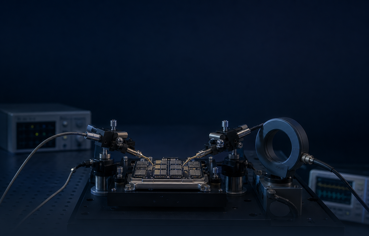
Support for SiC and GaN power device characterization, module validation, and gate-drive debugging with wide-bandwidth probes, precision current sensing, and stable measurement chains.
SiC and GaN devices switch at nanosecond speeds. Measurement chains need high bandwidth, fast response, and waveform fidelity.
Accurate loss measurement requires tightly synchronized voltage, current, and timing channels across the test setup.
Wide-bandgap test environments create strong dv/dt and electromagnetic noise. Stable probing and system-level grounding are essential.
As SiC and GaN adoption accelerates, test engineers face steeper requirements for switching-speed fidelity, timing accuracy, and noise immunity in device and module characterization.
Measurement tools must remain dependable under demanding development and validation conditions.
The measurement chain is designed for practical lab, production, and troubleshooting environments.
Selection guidance, usage support, and maintenance services help reduce lifecycle friction.
Validate turn-on, turn-off, reverse recovery, and switching losses for power device characterization.
Evaluate module behavior under high-voltage, high-frequency conditions with synchronized voltage and current measurements.
Observe gate-drive signals, voltage, and current waveforms to assess delay, oscillation, and protection behavior.
Maintain stable voltage and current measurement chains in strong-noise, high-switching-speed environments.